詳細(xì)介紹
LT210 Rev.A
Letex Technology Corp.
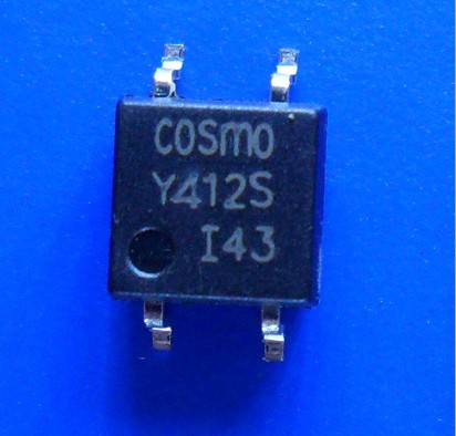
Photo DMOS-FET Relay
Description
The LT210 is a miniature 1-Form A solid state relay in a 4 pin SOP package that employs
optically coupled MOSFET technology to provide 1500V of input to output isolation.
The optically coupled input is controlled by a highly efficient GaAlAs infrared LED and
MOS FETs on the output side.
Features
?SOP package 4 Pin type in miniature design (4.4×4.3×2.0mm / .173×.169×.083inch)
?Low driver power requirements (TTL/CMOS Compatible)
?No moving parts
?High reliability
?Arc-Free with no snubbing circuits
?1500Vrms Input/Output isolation
?Tape & Reel version available
Applications
?Telecommunications (PC, Electronic notepad)
?Measuring and Testing equipment
?Industrial control
?Security equipments
?High speed inspection machine
Outline Dimensions
3
Unit : mm inch
Tolerance: 0.1 .004
1
4
2
1
2
4 3
1. LED Anode
2. LED Cathode
3, 4. Drain (MOS FET) LT210 Rev.A
Letex Technology Corp.
Photo DMOS-FET Relay Specifications
Part Name: LT210
(Load voltage: 400V / Load current: 100mA)
Absolute Maximum Ratings (Ambient Temperature: 25℃)
Item Symbol
Value Units Note
Input
Continuous LED Current I
F
50 mA
Peak LED Current I
FP
1000 mA
f=100Hz,
duty=1%
LED Reverse Voltage V
R
5 V
Input Power Dissipation P
In
75 mW
Output
Load Voltage V
L
400 V(AC peak or DC)
Load Current I
L
100 mA
Peak Load Current I
Peak
0.6 A 100ms(1 pulse)
Output Power Dissipation Pout 300 mW
Total Power Dissipation P
T
350 mW
I/O Breakdown Voltage V
I/O
1500 Vrms RH=60%, 1min
Operating Temperature T
Opr
-40 to +85
℃
Storage Temperature T
Stg
-40 to +100
℃
Pin Soldering Temperature T
Sol
260
℃
10 sec max.
Electrical Specifications (Ambient Temperature: 25℃)
Item Symbol
MIN.
TYP. MAX. Units
Conditions
Input
LED Forward Voltage V
F
1.2 1.4 V I
F
=10mA
Operation LED Current
I
F On
0.5 1.0 mA
Recovery LED Current
I
F Off
0.35 0.5 mA
Recovery LED Voltage V
F Off
0.7 V
Output
On-Resistance R
On
20 24
?
I
F
=5mA,I
L
=100mA,
Time to flow is within
1 sec.
Off-State Leakage
Current
I
Leak
1 uA
V
L
=Rating
Output Capacitance C
Ou
t 45 pF V
L
=0, f=1MHz
Transmis
sion
Turn-On Time T
On
0.23 0.5 ms I
F
=5mA, I
L
=100mA,
Turn-Off Time T
Of
f 0.03 0.2 ms
Coupled
I/O Isolation Resistance
R
I/O
1010
? DC500V
I/O Capacitance C
I/O
0.8 1.5 pF f=1MHz LT210 Rev.A
Letex Technology Corp.
Reference Data
LED foward current Vs.
turn off time characteristics
Voltage Vs. currennt characteristics
of output at MOS portion
10
0.2
0
0
0.4
0.6
0.8
LED forward current (mA)
20 30 40 50
0.02
60
0
0 10
0.04
0.06
0.08
LED forward current (mA)
20 30 40 50
LED foward current Vs.
turn on time characteristics
50mA
30mA
20mA
10mA
5mA
1.0
1.2
-40
0
-20
Ambient temperature (℃)
0 20 60 85 40
LED forward voltage Vs.
Ambient temperature
1.0
1.1
1.2
1.3
1.5
1.4
0.10
0.12
100
-100
-5 -4
1
-20
-80
-60
-40
-3 -2
20
-1
40
Voltage, V
2 3 4 5
80
60
100
LT210
LT211
150
50
60
0
0 10
50
100
Applied voltage (V)
20 40 30
Applied voltage Vs.
output capacitance characteristics
400
200
0
10-12
Load voltage (V)
10 -9
10 -6
10 -3
LT210
-40
0
-20
0.1
0.2
0.3
LT210
Ambient temperature (℃)
0 20 60 40
85
0.4
0.5
-40
0
-20
Turn off time Vs.
Ambient temperature
Ambient temperature (℃)
0 20 60 80 40
85
100 -40
0
-20
1
2
3
Ambient temperature (℃)
0 20 60 85 40
LED operate current Vs.
Ambient temperature
4
5
100 -40
0
-20
Ambient temperature (℃)
0 20 60 85 40
Load current Vs.
Ambient temperature
20
40
60
80
100
120
LT210
On resistance Vs.
Ambient temperature
30
10
20
40
50
100
100
100 -40
0
-20
0.2
0.4
0.6
Ambient temperature (℃)
20 0 40 60 85
LED turn off current Vs.
Ambient temperature
0.8
1.0
100
0
-40 -20
Ambient temperature (℃)
20 0 40 60 80
85
Turn on time Vs.
Ambient temperature
1.0
0.5
1.5
2.0
2.5
3.0
LT210
350300250200150100 50
Off state leakage current Vs.
Load voltage characteristics
Turn on time (ms)
Turn off time (ms)
LED forward voltage (V)
Current, A
Out capacitance (pF)
Off state leakage current (A)
Turn off time (ms)
LED operate current (mA)
Load current (mA)
On resistabce (Ω)
LED turn off time (mA)
Turn on time (ms)LT210 Rev.A
Letex Technology Corp.
Taping Specifications for Surface Mount Devices
Direction of feed
Unit : mm
Label sticking position
Unit : mm
Tolerance : ±0.1
Recommended Mounting Pad
(Top view)
Marking
(Each photo MOS Relay shall be marked
with the following information)
R963
LT210
LETEX
Brand Name
Part Name
Date Code
RoHS
Weeks
Year
Monthly
R963
Note: 1. There shall be leader of 230 mm minimum which may consist of carrier and or cover tape
follower by a minimum of 160 mm of carrier tape sealed with cover tape.
2. There shall be a minimum of 160 mm of empty component pockets sealed with cover tape.
3. Devices are pockets in accordance with EIA standard EIA-481-A and specifications given above.
4. Packaging: 2,000pcs per reel, 2 reel per box, 5 boxes per carton.
LT218
Rev.B
Letex Technology Corp.
Photo DMOS-FET Relay
Description
The LT218 is a miniature 1-Form A solid state relay in a 4 pin SOP package that employs
optically coupled MOSFET technology to provide 1500V of input to output isolation.
The optically coupled input is controlled by a highly efficient GaAlAs infrared LED and
MOS FETs on the output side.
Features
?SOP package 4 Pin type in miniature design (4.4×4.3×2.0mm / .173×.169×.083inch)
?Low driver power requirements (TTL/CMOS Compatible)
?No moving parts
?Hi-A : Load Current = 2.5A
?High reliability
?Arc-Free with no snubbing circuits
?1500Vrms Input/Output isolation
?Tape & Reel version available
Applications
?Telecommunications (PC, Electronic notepad)
?Measuring and Testing equipment
?Industrial control
?Security equipments
?High speed inspection machine
Outline Dimensions
3
Unit : mm inch
Tolerance: 0.1 .004
1
4
2
1
2
4 3
1. LED Anode
2. LED Cathode
3, 4. Drain (MOS FET) LT218
Rev.B
Letex Technology Corp.
Photo DMOS-FET Relay Specifications
Part Name: LT218
(Load voltage:40V / Load current: 2.5A)
Absolute Maximum Ratings (Ambient Temperature: 25℃)
Item Symbol
Value Units Note
Input
Continuous LED Current IF 50 mA
Peak LED Current IFP 1000 mA
f=100Hz,
duty=1%
LED Reverse Voltage VR 5 V
Input Power Dissipation PIn 75 mW
Output
Load Voltage VL 40 V(AC peak or DC)
Load Current IL 2.5 A
Peak Load Current IPeak 5.0 A
100ms(1 pulse)
Output Power Dissipation Pout 400 mW
Total Power Dissipation PT 500 mW
I/O Breakdown Voltage VI/O 1500 Vrms RH=60%, 1min
Operating Temperature Topr -40 to +85
℃
Storage Temperature Tstg -40 to +100
℃
Pin Soldering Temperature Tsol 260
℃
10 sec max.
Electrical Specifications (Ambient Temperature: 25℃)
Item Symbol
MIN.
TYP. MAX. Units
Conditions
Input
LED Forward Voltage VF 1.2 1.4 V IF=10mA
Operation LED Current
IFon 0.5 2.0 mA
Recovery LED Current
IFoff 0.35 0.5 mA
Recovery LED Voltage VFoff 0.7 V
Output
On-Resistance Ron 0.06 0.1
?
IF=5mA,IL=100mA,
Time to flow is within
1 sec.
Off-State Leakage
Current
ILeak 1 uA VL=Rating
Output Capacitance Cout 100 pF VL=0, f=1MHz
Transmis
sion
Turn-On Time Ton 0.5 1.0 ms IF=5mA, IL=100mA,
Turn-Off Time Toff 0.02 0.5 ms
Coupled
I/O Isolation Resistance
RI/O
1010
?
DC500V
I/O Capacitance CI/O 0.8 1.5 pF f=1MHz LT218
Rev.B
Letex Technology Corp.
Reference Data
LED foward current Vs.
turn off time characteristics
Voltage Vs. currennt characteristics
of output at MOS portion
10
0.2
0
0
0.4
0.6
0.8
LED forward current (mA)
20 30 40 50
0.02
60
0
0 10
0.04
0.06
0.08
LED forward current (mA)
20 30 40 50
LED foward current Vs.
turn on time characteristics
50mA
30mA
20mA
10mA
5mA
1.0
1.2
-40
0
-20
Ambient temperature (℃)
40
0 20 60 85
LED forward voltage Vs.
Ambient temperature
1.0
1.1
1.2
1.3
1.5
1.4
0.10
0.12
100
-10
-5 -4
1
-2
-8
-6
-4
-3 -2
2
-1
4
Voltage, V
2 3 4 5
8
6
10
150
50
60
0
0 10
50
100
Applied voltage (V)
30
20 40
Applied voltage Vs.
output capacitance characteristics
40
200
0
10-12
8
Load voltage (V)
24
16 32
10 -9
10 -6
10 -3
-40
0
-20
0.01
0.02
0.03
Ambient temperature (℃)
40
0 20 60 85
0.04
-40
0
-20
Turn off time Vs.
Ambient temperature
Ambient temperature (℃)
40
0 20 60 80
85
100 -40
0
-20
1
2
3
Ambient temperature (℃)
40
0 20 60 85
LED operate current Vs.
Ambient temperature
4
5
100 -40
0
-20
Ambient temperature (℃)
40
0 20 60 85
Load current Vs.
Ambient temperature
0.5
1.0
1.5
2.0
2.5
3.0
On resistance Vs.
Ambient temperature
100
100
100 -40
0
-20
0.2
0.4
0.6
Ambient temperature (℃)
20
0 40 60 85
LED turn off current Vs.
Ambient temperature
0.8
1.0
100
0
-40 -20
Ambient temperature (℃)
20
0 40 60 80
85
Turn on time Vs.
Ambient temperature
1.0
0.5
1.5
2.0
2.5
3.0
0.05
0.10
0.15
0.20
Off state leakage current Vs.
Load voltage characteristics
Turn on time (ms)
Turn off time (ms)
LED forward voltage (V)
Current, A
Out capacitance (pF)
Off state leakage current (A)
Turn off time (ms)
LED operate current (mA)
Load current (A)
On resistabce (Ω)
LED turn off time (mA)
Turn on time (ms)LT218
Rev.B
Letex Technology Corp.
Taping Specifications for Surface Mount Devices
Direction of feed
Unit : mm
Label sticking position
Unit : mm
Tolerance : ±0.1
Recommended Mounting Pad
(Top view)
Marking
(Each photo MOS Relay shall be marked
with the following information)
Brand Name
Part Name
Date Code
LETEX
LT218
R963
R963
RoHS
Weeks
Monthly
Year
Note: 1. There shall be leader of 230 mm minimum which may consist of carrier and or cover tape
follower by a minimum of 160 mm of carrier tape sealed with cover tape.
2. There shall be a minimum of 160 mm of empty component pockets sealed with cover tape.
3. Devices are pockets in accordance with EIA standard EIA-481-A and specifications given above.
4. Packaging: 2,000pcs per reel, 2 reel per box, 5 boxes per carton.
 內(nèi)容編輯

